SoylentNews is people
SoylentNews
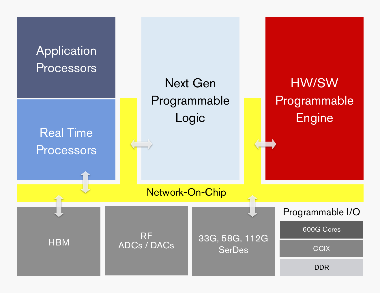
Xilinx Announces Project Everest: The 7nm FPGA SoC Hybrid
This week Xilinx is making public its latest internal project for the next era of specialized computing. The new product line, called Project Everest in the interim, is based around what Xilinx is calling an ACAP – an Adaptive Compute Acceleration Platform. The idea here is that for both compute and acceleration, particularly in the data center, the hardware has to be as agile as the software. Project Everest will combine Xilinx's highest performing next-generation programmable logic along with application processors, real-time processors, programmable engines, RF, high-speed SerDes, programmable IO, HBM, and a custom network-on-chip. The idea is that space typically devoted to hard blocks in FPGAs (such as memory controllers) are now optimized on chip, leaving more programmable silicon for the compute and adaptability. Project Everest is one of the Three Big Trends as identified by Xilinx's new CEO, Victor Peng.
[...] Xilinx's ACAP portfolio will be initiated with TSMC's 7nm manufacturing process, with the first tapeouts due in late 2018. Xilinx states that Project Everest has been a monumental internal effort, taking 4-5 years and 1500 engineers already, with over $1b in R&D costs. The final big chips are expected to weigh in at 50 billion transistors, with a mix of monolithic and interposer designs based on configurations.
Today's announcement is more of a teaser than anything else – the diagram above is about the limit to which that Xilinx will talk about features and the product portfolio. The value of the ACAP, according to Xilinx, will be its feature set and millisecond-level configurability. For a server on the edge, for example, an ACAP can use both the programmable logic elements for millisecond bitstream reconfiguration of different processes along with the application processors for general logic or the programmable engines as ASIC-level acceleration. This can lead to, among other things, different AI acceleration techniques and 5G RF manageability by multiple containers/VMs on a single ACAP. The overriding idea is that the ACAP can apply dynamic optimization for workloads, with Xilinx citing a 10-100x speedup over CPUs and more use cases than GPUs or ASICs as a fundamental value to the new hardware, built through software and hardware programmability. Xilinx also stated that the RF will have four times the bandwidth of current 16nm radios, leveraging 16x16 800 MHz radios.
Also at The Register and The Next Platform.
(Score: 3, Informative) by bob_super on Thursday March 22 2018, @01:46AM
GPUs almost always talk to a host via PCIe. FPGAs typically get their data straight from the pipe (Video, Ethernet, fibre channel...), saving the whole CPU loop, helping tremendously in real-time applications.
Also, GPUs are fundamentally an array of little processors specialized in crunching parallel math instructions, with some controls and loops, and uploading results back to a memory. They're the best at what they do. FPGAs, on the other hand, crunch data at lower clocks, but pretty much every single clock tick (some blocks have minor latencies), and can merge and split memories and datastreams in real time with high precision, creating standard-complaint streams and other wholistic behaviors which a CPU or GPU is ill-fitted for.
It's hard to summarize in one post. You can't crunch the content of a 400Gig-E pipe with a GPU. That doesn't takes an insane FPGA (the biggest can do multiple 400GE), and it will do it within a tolerable thermal envelope, though for a pretty high price (which typically doesn't matter if you have to crunch a 400G pipe).
Fundamentally, it's the difference between sequential and heavily parallelized programming (CPU/GPU) versus concurrent programming (FPGA/ASIC). Every piece of data in the FPGA could be processed with every clock cycle (typically not, but every flop's input is evaluated at every tick). A CPU/GPU will grab one chunk of data (one register, maybe a SIMD), move it to process, then push it back, then grab the next one, heavily pipelined, but still nowhere near the less-flexible super-efficiency of an ASIC dataflow (and an ASIC is just an optimized frozen FPGA).