SoylentNews is people
SoylentNews
Samsung has announced the mass production of dynamic random access memory (DRAM) packages using the second generation High Bandwidth Memory (HBM2) interface.
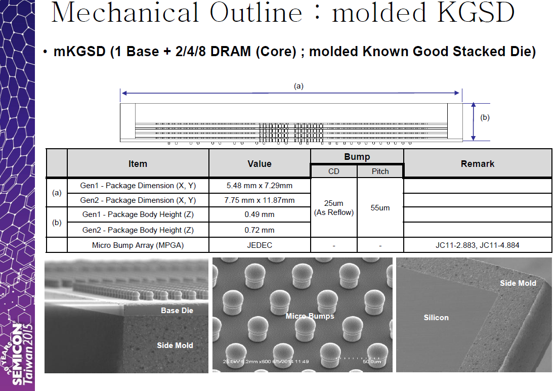
AMD was the first and only company to introduce products using HBM1. AMD's Radeon R9 Fury X GPUs featured 4 gigabytes of HBM1 using four 1 GB packages. Both AMD and Nvidia will introduce GPUs equipped with HBM2 memory this year. Samsung's first HBM2 packages will contain 4 GB of memory each, and the press release states that Samsung intends to manufacture 8 GB HBM2 packages within the year. GPUs could include 8 GB of HBM2 using half of the die space used by AMD's Fury X, or just one-quarter of the die space if 8 GB HBM2 packages are used next year. Correction: HBM2 packages may be slightly physically larger than HBM1 packages. For example, SK Hynix will produce a 7.75 mm × 11.87 mm (91.99 mm2) HBM2 package, compared to 5.48 mm × 7.29 mm (39.94 mm2) HBM1 packages.
The 4GB HBM2 package is created by stacking a buffer die at the bottom and four 8-gigabit (Gb) core dies on top. These are then vertically interconnected by TSV holes and microbumps. A single 8Gb HBM2 die contains over 5,000 TSV holes, which is more than 36 times that of a 8Gb TSV DDR4 die, offering a dramatic improvement in data transmission performance compared to typical wire-bonding based packages.
Samsung's new DRAM package features 256GBps of bandwidth, which is double that of a HBM1 DRAM package. This is equivalent to a more than seven-fold increase over the 36GBps bandwidth of a 4Gb GDDR5 DRAM chip, which has the fastest data speed per pin (9Gbps) among currently manufactured DRAM chips. Samsung's 4GB HBM2 also enables enhanced power efficiency by doubling the bandwidth per watt over a 4Gb-GDDR5-based solution, and embeds ECC (error-correcting code) functionality to offer high reliability.
TSV refers to through-silicon via, a vertical electrical connection used to build 3D chip packages such as High Bandwidth Memory.
Update: HBM2 has been formalized in JEDEC's JESD235A standard, and Anandtech has an article with additional technical details.
Previously:
AMD Teases x86 Improvements, High Bandwidth Memory GPUs
AMD Shares More Details on High Bandwidth Memory
Samsung Mass Produces 128 GB DDR4 Server Memory
(Score: 0) by Anonymous Coward on Wednesday January 20 2016, @06:08PM
Given that rowhammer is a thing now. Do want ECC.
(Score: 4, Funny) by GungnirSniper on Wednesday January 20 2016, @06:09PM
Enough horsepower to play Crysis.
Tips for better submissions to help our site grow. [soylentnews.org]
(Score: 2) by takyon on Wednesday January 20 2016, @06:49PM
I find it neat that if AMD keeps the same amount of die space for memory as was used in the Fury models, the new cards would have 16 GB rather than 4 GB of RAM. I'm guessing they will cut it to 8 GB instead.
[SIG] 10/28/2017: Soylent Upgrade v14 [soylentnews.org]
(Score: 2) by VLM on Wednesday January 20 2016, @06:49PM
So I look over at a PCB with 800 or so vias and
over 5,000 TSV holes
over 5000 things to go wrong... ouch. Well I guess if yields are high enough, its not my problem.
I imagine they provision these things with massive extra capacity and block out the 20% of the die that doesn't work but still... Wow time.
(Score: 2) by takyon on Wednesday January 20 2016, @07:03PM
I'm willing to massively cling to this explanation.
This is the second generation of High Bandwidth Memory and the details [kitguru.net] have been known for months. We don't even know what HBM3 will look like.
[SIG] 10/28/2017: Soylent Upgrade v14 [soylentnews.org]
(Score: 2) by shortscreen on Wednesday January 20 2016, @06:57PM
maybe it's time for CPU designers to bump up the cache line size again
(Score: 2) by RamiK on Wednesday January 20 2016, @09:35PM
I think I was talking about quantum computing last time I brought it up, but I think even at theses speeds it might be time to consider putting a kernel and garbage collector in a micro-controller.
compiling...
(Score: 3, Interesting) by jasassin on Wednesday January 20 2016, @09:11PM
What does this mean? Where is the bottleneck now?
jasassin@gmail.com GPG Key ID: 0xE6462C68A9A3DB5A
(Score: 2, Insightful) by RamiK on Wednesday January 20 2016, @09:25PM
Same as it ever was forever: The stupid meatbag clicking mechanical buttons for output and reading input at a few bauds at most per char.
compiling...
(Score: 4, Informative) by takyon on Thursday January 21 2016, @12:52AM
On the GPU front, if we assume AMD and Nvidia uses a minimum of 8 GB of HBM2 going forward, there shouldn't really be a VRAM bottleneck for most users (parallel computing users maybe, after all, Nvidia Titan X comes with 12 GB of VRAM).
GPUs with HBM instead of GDDR5 can have a lower TDP, or use more power elsewhere, the opposite of a bottleneck.
AMD's APUs (combining CPU with integrated GPU) are apparently bottlenecked by memory bandwidth, and AMD plans to add HBM to some future APUs. That will increase their cost but graphics performance should go up.
http://www.eurogamer.net/articles/digitalfoundry-2015-amd-reveals-hbm-future-of-graphics-ram-tech [eurogamer.net]
http://www.anandtech.com/show/9390/the-amd-radeon-r9-fury-x-review/6 [anandtech.com]
[SIG] 10/28/2017: Soylent Upgrade v14 [soylentnews.org]