Samsung has announced the mass production of dynamic random access memory (DRAM) packages using the second generation High Bandwidth Memory (HBM2) interface.
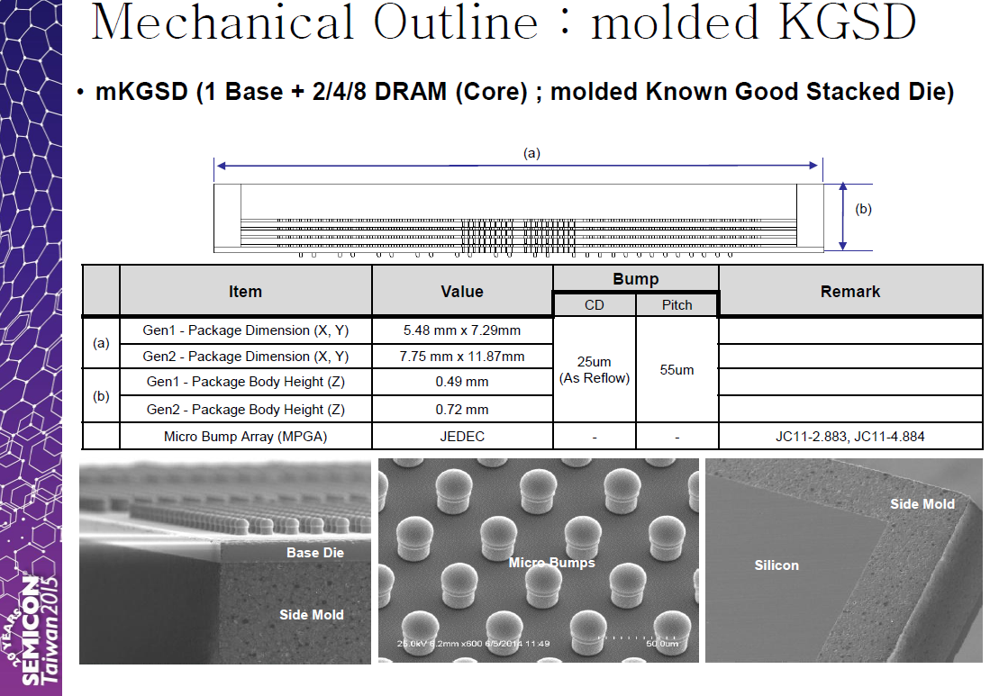
AMD was the first and only company to introduce products using HBM1. AMD's Radeon R9 Fury X GPUs featured 4 gigabytes of HBM1 using four 1 GB packages. Both AMD and Nvidia will introduce GPUs equipped with HBM2 memory this year. Samsung's first HBM2 packages will contain 4 GB of memory each, and the press release states that Samsung intends to manufacture 8 GB HBM2 packages within the year. GPUs could include 8 GB of HBM2 using half of the die space used by AMD's Fury X, or just one-quarter of the die space if 8 GB HBM2 packages are used next year. Correction: HBM2 packages may be slightly physically larger than HBM1 packages. For example, SK Hynix will produce a 7.75 mm × 11.87 mm (91.99 mm2) HBM2 package, compared to 5.48 mm × 7.29 mm (39.94 mm2) HBM1 packages.
The 4GB HBM2 package is created by stacking a buffer die at the bottom and four 8-gigabit (Gb) core dies on top. These are then vertically interconnected by TSV holes and microbumps. A single 8Gb HBM2 die contains over 5,000 TSV holes, which is more than 36 times that of a 8Gb TSV DDR4 die, offering a dramatic improvement in data transmission performance compared to typical wire-bonding based packages.
Samsung's new DRAM package features 256GBps of bandwidth, which is double that of a HBM1 DRAM package. This is equivalent to a more than seven-fold increase over the 36GBps bandwidth of a 4Gb GDDR5 DRAM chip, which has the fastest data speed per pin (9Gbps) among currently manufactured DRAM chips. Samsung's 4GB HBM2 also enables enhanced power efficiency by doubling the bandwidth per watt over a 4Gb-GDDR5-based solution, and embeds ECC (error-correcting code) functionality to offer high reliability.
TSV refers to through-silicon via, a vertical electrical connection used to build 3D chip packages such as High Bandwidth Memory.
Update: HBM2 has been formalized in JEDEC's JESD235A standard, and Anandtech has an article with additional technical details.
Previously:
AMD Teases x86 Improvements, High Bandwidth Memory GPUs
AMD Shares More Details on High Bandwidth Memory
Samsung Mass Produces 128 GB DDR4 Server Memory
Related Stories
Today was Advanced Micro Devices' (AMD) 2015 Financial Analyst Day. The last one was held in 2012. Since then, the company has changed leadership, put its APUs in the major consoles, and largely abandoned the high-end chip market to Intel. Now AMD says it is focusing on gaming, virtual reality, and datacenters. AMD has revealed details of upcoming CPUs and GPUs at the event:
Perhaps the biggest announcement relates to AMD's x86 Zen CPUs, coming in 2016. AMD is targeting a 40% increase in instructions-per-clock (IPC) with Zen cores. By contrast, Intel's Haswell (a "Tock") increased IPC by about 10-11%, and Broadwell (a "Tick") increased IPC by about 5-6%. AMD is also abandoning the maligned Bulldozer modules with Clustered Multithreading in favor of a Simultaneous Multithreading design, similar to Intel's Hyperthreading. Zen is a high priority for AMD to the extent that it is pushing back its ARM K12 chips to 2017. AMD is also shifting focus away from Project Skybridge, an "ambidextrous framework" that combined x86 and ARM cores in SoCs. Zen cores will target a wide range of designs from "top-to-bottom", including both sub-10W TDPs and up to 100W. The Zen architecture will be followed by Zen+ at some point.
On the GPU front, AMD's 2016 GPUs will use FinFETs. AMD plans to be the first vendor to use High Bandwidth Memory (HBM), a 3D/stacked memory standard that enables much higher bandwidth (hence the name) and saves power. NVIDIA also plans to use HBM in its Pascal GPUs slated for 2016. The HBM will be positioned around the processor, as the GPU's thermal output would make cooling the RAM difficult if it were on top. HBM is competing against the similar Hybrid Memory Cube (HMC) standard.
Advanced Micro Devices (AMD) has shared more details about the High Bandwidth Memory (HBM) in its upcoming GPUs.
HBM in a nutshell takes the wide & slow paradigm to its fullest. Rather than building an array of high speed chips around an ASIC to deliver 7Gbps+ per pin over a 256/384/512-bit memory bus, HBM at its most basic level involves turning memory clockspeeds way down – to just 1Gbps per pin – but in exchange making the memory bus much wider. How wide? That depends on the implementation and generation of the specification, but the examples AMD has been showcasing so far have involved 4 HBM devices (stacks), each featuring a 1024-bit wide memory bus, combining for a massive 4096-bit memory bus. It may not be clocked high, but when it's that wide, it doesn't need to be.
AMD will be the only manufacturer using the first generation of HBM, and will be joined by NVIDIA in using the second generation in 2016. HBM2 will double memory bandwidth over HBM1. The benefits of HBM include increased total bandwidth (from 320 GB/s for the R9 290X to 512 GB/s in AMD's "theoretical" 4-stack example) and reduced power consumption. Although HBM1's memory bandwidth per watt is tripled compared to GDDR5, the memory in AMD's example uses a little less than half the power (30 W for the R9 290X down to 14.6 W) due to the increased bandwidth. HBM stacks will also use 5-10% as much area of the GPU to provide the same amount of memory that GDDR5 would. That could potentially halve the size of the GPU:
By AMD's own estimate, a single HBM-equipped GPU package would be less than 70mm × 70mm (4900mm2), versus 110mm × 90mm (9900mm2) for R9 290X.
HBM will likely be featured in high-performance computing GPUs as well as accelerated processing units (APUs). HotHardware reckons that Radeon 300-series GPUs featuring HBM will be released in June.
Samsung has developed the world's first 128 GB DDR4 registered memory modules for servers. From the press release:
Following Samsung's introduction of the world-first 3D TSV DDR4 DRAM (64GB) in 2014, the company's new TSV registered dual inline memory module (RDIMM) marks another breakthrough that opens the door for ultra-high capacity memory at the enterprise level. Samsung's new TSV DRAM module boasts the largest capacity and the highest energy efficiency of any DRAM modules today, while operating at high speed and demonstrating excellent reliability.
From The Register:
The Register is aware of servers with 96 DIMM slots, which means ... WOAH! ... 12.2 terabytes of RAM in a single server if you buy Samsung's new babies.
Samsung says these new DIMMS are special because "the chip dies are ground down to a few dozen micrometers, pierced with hundreds of fine holes and vertically connected by electrodes passing through the holes, allowing for a significant boost in signal transmission."
There's also "a special design through which the master chip of each 4GB package embeds the data buffer function to optimise module performance and power consumption."
JEDEC has finalized the GDDR5X SGRAM specification:
The new technology is designed to improve bandwidth available to high-performance graphics processing units without fundamentally changing the memory architecture of graphics cards or memory technology itself, similar to other generations of GDDR, although these new specifications are arguably pushing the phyiscal[sic] limits of the technology and hardware in its current form. The GDDR5X SGRAM (synchronous graphics random access memory) standard is based on the GDDR5 technology introduced in 2007 and first used in 2008. The GDDR5X standard brings three key improvements to the well-established GDDR5: it increases data-rates by up to a factor of two, it improves energy efficiency of high-end memory, and it defines new capacities of memory chips to enable denser memory configurations of add-in graphics boards or other devices. What is very important for developers of chips and makers of graphics cards is that the GDDR5X should not require drastic changes to designs of graphics cards, and the general feature-set of GDDR5 remains unchanged (and hence why it is not being called GDDR6).
[...] The key improvement of the GDDR5X standard compared to the predecessor is its all-new 16n prefetch architecture, which enables up to 512 bit (64 Bytes) per array read or write access. By contrast, the GDDR5 technology features 8n prefetch architecture and can read or write up to 256 bit (32 Bytes) of data per cycle. Doubled prefetch and increased data transfer rates are expected to double effective memory bandwidth of GDDR5X sub-systems. However, actual performance of graphics cards will depend not just on DRAM architecture and frequencies, but also on memory controllers and applications. Therefore, we will need to test actual hardware to find out actual real-world benefits of the new memory.
What purpose does GDDR5X serve if superior 1st and 2nd generation High Bandwidth Memory (HBM) are around? GDDR5X memory will be cheaper than HBM and its use is more of an evolutionary than revolutionary change from existing GDDR5-based hardware.
During a keynote at GTC 2016, Nvidia announced the Tesla P100, a 16nm FinFET Pascal graphics processing unit with 15.3 billion transistors intended for high performance and cloud computing customers. The GPU includes 16 GB of High Bandwidth Memory 2.0 with 720 GB/s of memory bandwidth and a unified memory architecture. It also uses the proprietary NVLink, an interconnect with 160 GB/s of bandwidth, rather than the slower PCI-Express.
Nvidia claims the Tesla P100 will reach 5.3 teraflops of FP64 (double precision) performance, along with 10.6 teraflops of FP32 and 21.2 teraflops of FP16. 3584 of a maximum possible 3840 stream processors are enabled on this version of the GP100 die.
At the keynote, Nvidia also announced a 170 teraflops (FP16) "deep learning supercomputer" or "datacenter in a box" called DGX-1. It contains eight Tesla P100s and will cost $129,000. The first units will be going to research institutions such as the Massachusetts General Hospital.
SK Hynix will begin mass production of 4 GB HBM2 memory stacks soon:
SK Hynix has quietly added its HBM Gen 2 memory stacks to its public product catalog earlier this month, which means that the start of mass production should be imminent. The company will first offer two types of new memory modules with the same capacity, but different transfer-rates, targeting graphics cards, HPC accelerators and other applications. Over time, the HBM2 family will get broader.
SK Hynix intends to initially offer its clients 4 GB HBM2 4Hi stack KGSDs (known good stack dies) based on 8 Gb DRAM devices. The memory devices will feature a 1024-bit bus as well as 1.6 GT/s (H5VR32ESM4H-12C) and 2.0 GT/s (H5VR32ESM4H-20C) data-rates, thus offering 204 GB/s and 256 GB/s peak bandwidth per stack.
Samsung has already manufactured 4 GB stacks. Eventually, there will also be 2 GB and 8 GB stacks available.
Previously: AMD Shares More Details on High Bandwidth Memory
Samsung Announces Mass Production of HBM2 DRAM
SK Hynix is almost ready to produce GDDR6 memory with higher than expected per-pin bandwidth:
In a surprising move, SK Hynix has announced its first memory chips based on the yet-unpublished GDDR6 standard. The new DRAM devices for video cards have capacity of 8 Gb and run at 16 Gbps per pin data rate, which is significantly higher than both standard GDDR5 and Micron's unique GDDR5X format. SK Hynix plans to produce its GDDR6 ICs in volume by early 2018.
GDDR5 memory has been used for top-of-the-range video cards for over seven years, since summer 2008 to present. Throughout its active lifespan, GDDR5 increased its data rate by over two times, from 3.6 Gbps to 9 Gbps, whereas its per chip capacities increased by 16 times from 512 Mb to 8 Gb. In fact, numerous high-end graphics cards, such as NVIDIA's GeForce GTX 1060 and 1070, still rely on the GDDR5 technology, which is not going anywhere even after the launch of Micron's GDDR5X with up to 12 Gbps data rate per pin in 2016. As it appears, GDDR6 will be used for high-end graphics cards starting in 2018, just two years after the introduction of GDDR5X.
Previously: Samsung Announces Mass Production of HBM2 DRAM
DDR5 Standard to be Finalized by JEDEC in 2018
In response to increased demand, Samsung is increasing production of the densest HBM2 DRAM available:
Samsung on Tuesday announced that it is increasing production volumes of its 8 GB, 8-Hi HBM2 DRAM stacks due to growing demand. In the coming months the company's 8 GB HBM2 chips will be used for several applications, including those for consumers, professionals, AI, as well as for parallel computing. Meanwhile, AMD's Radeon Vega graphics cards for professionals and gamers will likely be the largest consumers of HBM2 in terms of volume. And while AMD is traditionally a SK Hynix customer, the timing of this announcement with AMD's launches certainly suggests that AMD is likely a Samsung customer this round as well.
Samsung's 8 GB HBM Gen 2 memory KGSDs (known good stacked die) are based on eight 8-Gb DRAM devices in an 8-Hi stack configuration. The memory components are interconnected using TSVs and feature over 5,000 TSV interconnects each. Every KGSD has a 1024-bit bus and offers up to 2 Gbps data rate per pin, thus providing up to 256 GB/s of memory bandwidth per single 8-Hi stack. The company did not disclose power consumption and heat dissipation of its HBM memory components, but we have reached out [to] Samsung for additional details.
Previously:
Samsung Announces Mass Production of HBM2 DRAM
CES 2017: AMD Vega GPUs and FreeSync 2
AMD Launches the Radeon Vega Frontier Edition
(Score: 0) by Anonymous Coward on Wednesday January 20 2016, @06:08PM
Given that rowhammer is a thing now. Do want ECC.
(Score: 4, Funny) by GungnirSniper on Wednesday January 20 2016, @06:09PM
Enough horsepower to play Crysis.
Tips for better submissions to help our site grow. [soylentnews.org]
(Score: 2) by takyon on Wednesday January 20 2016, @06:49PM
I find it neat that if AMD keeps the same amount of die space for memory as was used in the Fury models, the new cards would have 16 GB rather than 4 GB of RAM. I'm guessing they will cut it to 8 GB instead.
[SIG] 10/28/2017: Soylent Upgrade v14 [soylentnews.org]
(Score: 2) by VLM on Wednesday January 20 2016, @06:49PM
So I look over at a PCB with 800 or so vias and
over 5,000 TSV holes
over 5000 things to go wrong... ouch. Well I guess if yields are high enough, its not my problem.
I imagine they provision these things with massive extra capacity and block out the 20% of the die that doesn't work but still... Wow time.
(Score: 2) by takyon on Wednesday January 20 2016, @07:03PM
I'm willing to massively cling to this explanation.
This is the second generation of High Bandwidth Memory and the details [kitguru.net] have been known for months. We don't even know what HBM3 will look like.
[SIG] 10/28/2017: Soylent Upgrade v14 [soylentnews.org]
(Score: 2) by shortscreen on Wednesday January 20 2016, @06:57PM
maybe it's time for CPU designers to bump up the cache line size again
(Score: 2) by RamiK on Wednesday January 20 2016, @09:35PM
I think I was talking about quantum computing last time I brought it up, but I think even at theses speeds it might be time to consider putting a kernel and garbage collector in a micro-controller.
compiling...
(Score: 3, Interesting) by jasassin on Wednesday January 20 2016, @09:11PM
What does this mean? Where is the bottleneck now?
jasassin@gmail.com GPG Key ID: 0xE6462C68A9A3DB5A
(Score: 2, Insightful) by RamiK on Wednesday January 20 2016, @09:25PM
Same as it ever was forever: The stupid meatbag clicking mechanical buttons for output and reading input at a few bauds at most per char.
compiling...
(Score: 4, Informative) by takyon on Thursday January 21 2016, @12:52AM
On the GPU front, if we assume AMD and Nvidia uses a minimum of 8 GB of HBM2 going forward, there shouldn't really be a VRAM bottleneck for most users (parallel computing users maybe, after all, Nvidia Titan X comes with 12 GB of VRAM).
GPUs with HBM instead of GDDR5 can have a lower TDP, or use more power elsewhere, the opposite of a bottleneck.
AMD's APUs (combining CPU with integrated GPU) are apparently bottlenecked by memory bandwidth, and AMD plans to add HBM to some future APUs. That will increase their cost but graphics performance should go up.
http://www.eurogamer.net/articles/digitalfoundry-2015-amd-reveals-hbm-future-of-graphics-ram-tech [eurogamer.net]
http://www.anandtech.com/show/9390/the-amd-radeon-r9-fury-x-review/6 [anandtech.com]
[SIG] 10/28/2017: Soylent Upgrade v14 [soylentnews.org]