In response to increased demand, Samsung is increasing production of the densest HBM2 DRAM available:
Samsung on Tuesday announced that it is increasing production volumes of its 8 GB, 8-Hi HBM2 DRAM stacks due to growing demand. In the coming months the company's 8 GB HBM2 chips will be used for several applications, including those for consumers, professionals, AI, as well as for parallel computing. Meanwhile, AMD's Radeon Vega graphics cards for professionals and gamers will likely be the largest consumers of HBM2 in terms of volume. And while AMD is traditionally a SK Hynix customer, the timing of this announcement with AMD's launches certainly suggests that AMD is likely a Samsung customer this round as well.
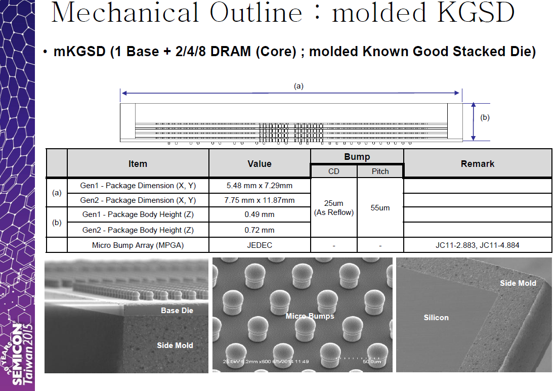
Samsung's 8 GB HBM Gen 2 memory KGSDs (known good stacked die) are based on eight 8-Gb DRAM devices in an 8-Hi stack configuration. The memory components are interconnected using TSVs and feature over 5,000 TSV interconnects each. Every KGSD has a 1024-bit bus and offers up to 2 Gbps data rate per pin, thus providing up to 256 GB/s of memory bandwidth per single 8-Hi stack. The company did not disclose power consumption and heat dissipation of its HBM memory components, but we have reached out [to] Samsung for additional details.
Previously:
Samsung Announces Mass Production of HBM2 DRAM
CES 2017: AMD Vega GPUs and FreeSync 2
AMD Launches the Radeon Vega Frontier Edition
Related Stories
Samsung has announced the mass production of dynamic random access memory (DRAM) packages using the second generation High Bandwidth Memory (HBM2) interface.
AMD was the first and only company to introduce products using HBM1. AMD's Radeon R9 Fury X GPUs featured 4 gigabytes of HBM1 using four 1 GB packages. Both AMD and Nvidia will introduce GPUs equipped with HBM2 memory this year. Samsung's first HBM2 packages will contain 4 GB of memory each, and the press release states that Samsung intends to manufacture 8 GB HBM2 packages within the year. GPUs could include 8 GB of HBM2 using half of the die space used by AMD's Fury X, or just one-quarter of the die space if 8 GB HBM2 packages are used next year. Correction: HBM2 packages may be slightly physically larger than HBM1 packages. For example, SK Hynix will produce a 7.75 mm × 11.87 mm (91.99 mm2) HBM2 package, compared to 5.48 mm × 7.29 mm (39.94 mm2) HBM1 packages.
The 4GB HBM2 package is created by stacking a buffer die at the bottom and four 8-gigabit (Gb) core dies on top. These are then vertically interconnected by TSV holes and microbumps. A single 8Gb HBM2 die contains over 5,000 TSV holes, which is more than 36 times that of a 8Gb TSV DDR4 die, offering a dramatic improvement in data transmission performance compared to typical wire-bonding based packages.
Samsung's new DRAM package features 256GBps of bandwidth, which is double that of a HBM1 DRAM package. This is equivalent to a more than seven-fold increase over the 36GBps bandwidth of a 4Gb GDDR5 DRAM chip, which has the fastest data speed per pin (9Gbps) among currently manufactured DRAM chips. Samsung's 4GB HBM2 also enables enhanced power efficiency by doubling the bandwidth per watt over a 4Gb-GDDR5-based solution, and embeds ECC (error-correcting code) functionality to offer high reliability.
TSV refers to through-silicon via, a vertical electrical connection used to build 3D chip packages such as High Bandwidth Memory.
Update: HBM2 has been formalized in JEDEC's JESD235A standard, and Anandtech has an article with additional technical details.
Previously:
AMD Teases x86 Improvements, High Bandwidth Memory GPUs
AMD Shares More Details on High Bandwidth Memory
Samsung Mass Produces 128 GB DDR4 Server Memory
AMD's Vega GPUs will be launching during the first half of 2017 (in 3-5 months). While AMD's previous Polaris chips were aimed at mainstream segments, AMD will aim for higher performance enthusiast users with Vega. Vega's next-generation compute unit will allow more lower precision instructions per clock cycle, such as FP16 and INT8 operations. The GPUs will also include High Bandwidth Memory 2.0. HBM2 allows up to 8 GB of DRAM per stack rather than the 1 GB limit imposed by HBM1 (used in AMD's Fury GPUs).
AMD has also announced FreeSync 2 for variable refresh displays, which apparently has more to do with high dynamic range (HDR) color than screen tearing and frame latency:
Trying to explain FreeSync 2 can get a bit tricky. Unlike the original FreeSync that it takes its name from, it's a multi-faceted technology: it's not just variable refresh, instead it's HDR as well. But it's also a business/platform play in a different way than FreeSync was. And while strictly speaking it's a superset of FreeSync, it is not meant to replace FreeSync wholesale. Perhaps the best way to think of FreeSync 2 is that it's a second, parallel initiative that is focused on what AMD, its monitor partners, and its game development partners can do to improve the state of high-end monitors and gaming.
In terms of features then, what is easily the cornerstone feature of [FreeSync 2] – and really its reason to be – is improving support for HDR gaming under Windows. As our own Brandon Chester has discussed more than once, the state of support for next-generation display technologies under Windows is mixed at best. HiDPI doesn't work quite as well as anyone would like it to, and there isn't a comprehensive & consistent color management solution to support monitors that offer HDR and/or color spaces wider than sRGB. The Windows 10 Anniversary Update has improved on the latter, but AMD is still not satisfied with the status quo on Windows 10 (never mind all the gamers still on Windows 7/8). As a result FreeSync 2 is, in part, their effort to upend the whole system and do better.
FreeSync 2 also at Tom's Hardware.
First it was unveiled, now it has launched. AMD has launched the Radeon Vega Frontier Edition at $999 for the air-cooled version and $1499 for liquid-cooled. The High Bandwidth Memory 2.0 included has been confirmed to be two stacks of 8-layer 8 GB HBM:
After what appears to be a very unusual false start, AMD has now formally launched their new Radeon Vega Frontier Edition card. First announced back in mid-May, the unusual card, which AMD is all but going out of their way to dissuade their usual consumer base from buying, will be available today for $999. Meanwhile its liquid cooled counterpart, which was also announced at the time, will be available later on in Q3 for $1499.
Interestingly, both of these official prices are some $200-$300 below the prices first listed by SabrePC two weeks ago in the false start. To date AMD hasn't commented on what happened there, however it's worth noting that SabrePC is as of press time still listing the cards for their previous prices, with both cards reporting as being in-stock.
[...] Feeding the GPU is AMD's previously announced dual stack HBM2 configuration, which is now confirmed to be a pair of 8 layer, 8GB "8-Hi" stacks. AMD has the Vega FE's memory clocked at just under 1.9Gbps, which gives the card a total memory bandwidth of 483GB/sec. And for anyone paying close attention to AMD's naming scheme here, they are officially calling this "HBC" memory – a callback to Vega's High Bandwidth Cache design.
IC Insights has predicted that DRAM prices will continue to increase this year:
According to IC Insights, DRAM prices will continue to increase even though they have more than doubled (+111%) over the last 12 months. IC Insights predicts that by the end of the calendar year DRAM's price per bit will have jumped a record 40% (or more).
[...] Of course, the record pricing levels are great for our friends at the major foundries. Samsung, Micron, and Sk Hynix are also raking in their own record profits and enjoying healthy margins. We have both DRAM and NAND shortages occurring at the same time, which is great for the foundries, and unless a player breaks ranks to gain market share, we can expect more foot-dragging before any of the foundries increases output.
The booming mobile industry and server markets are exacerbating the issue, so you would expect that the fabs would boost DRAM output. Unfortunately, the three primary fabs (Micron bought Elpida, reducing the number of players) don't share the same vision.
IC Insights indicates that Micron will not increase production capacity, instead relying upon improvements in yields and shrinking down to smaller nodes to boost its DRAM bit output. Sk Hynix has expressed its desire to boost DRAM output but hasn't set a firm timeline for fab expansion (unlikely to occur in the near term). Samsung is as tight-lipped as usual, so we aren't sure of its intentions.
In the 1980s there were 23 major DRAM suppliers, but cutthroat pricing and continual oversupplies eventually led to the wave of consolidation that left us with the current three suppliers.
Previously:
December 2015: DDR4 Memory Prices Declined 40% in 6 Months
May 2017:
DRAM Price Surge Continues
Samsung Set to Outpace Intel in Semiconductor Revenues
July 2017:
Micron Temporarily Suspends Operation of DRAM Production Facility
Samsung Increases Production of 8 GB High Bandwidth Memory 2.0 Stacks
August 2017:
DRAM Prices Continue to Climb
Samsung & SK Hynix Graphics Memory Prices Increase Over 30% In August
Intel squeezed an AMD graphics chip, RAM and CPU into one module
the new processor integrates a "semi-custom" AMD graphics chip and the second generation of Intel's "High Bandwidth Memory (HBM2)", which is comparable to GDDR5 in a traditional laptop.
Intel CPU and AMD GPU, together at last
Summary of Intel's news:
The new product, which will be part of our 8th Gen Intel Core family, brings together our high-performing Intel Core H-series processor, second generation High Bandwidth Memory (HBM2) and a custom-to-Intel third-party discrete graphics chip from AMD's Radeon Technologies Group* – all in a single processor package.
[...] At the heart of this new design is EMIB (Embedded Multi-Die Interconnect Bridge), a small intelligent bridge that allows heterogeneous silicon to quickly pass information in extremely close proximity. EMIB eliminates height impact as well as manufacturing and design complexities, enabling faster, more powerful and more efficient products in smaller sizes. This is the first consumer product that takes advantage of EMIB.
[...] Additionally, this solution is the first mobile PC to use HBM2, which consumes much less power and takes up less space compared to traditional discrete graphics-based designs using dedicated graphics memory, like GDDR5 memory.
takyon: This is more like an "integrated discrete GPU" than standard integrated graphics. It also avoids the need for Intel to license AMD's IP. AMD also needs to make a lot of parts since its wafer supply agreement with GlobalFoundries penalizes AMD if they buy less than a target number of wafers each year.
Also at AnandTech and Ars Technica.
Previously: AMD Stock Surges on Report of Intel Graphics Licensing Deal, 16-Core Ryzen Confirmed
Related: Samsung Increases Production of 8 GB High Bandwidth Memory 2.0 Stacks
Samsung's second generation ("1y-nm") 8 Gb DDR4 DRAM dies are being mass produced:
Samsung late on Wednesday said that it had initiated mass production of DDR4 memory chips using its second generation '10 nm-class' fabrication process. The new manufacturing technology shrinks die size of the new DRAM chips and improves their performance as well as energy efficiency. To do that, the process uses new circuit designs featuring air spacers (for the first time in DRAM industry). The new DRAM ICs (integrated circuits) can operate at 3600 Mbit/s per pin data rate (DDR4-3600) at standard DDR4 voltages and have been validated with major CPU manufacturers already.
[...] Samsung's new DDR4 chip produced using the company's 1y nm fabrication process has an 8-gigabit capacity and supports 3600 MT/s data transfer rate at 1.2 V. The new D-die DRAM runs 12.5% faster than its direct predecessor (known as Samsung C-die, rated for 3200 MT/s) and is claimed to be up to 15% more energy efficient as well. In addition, the latest 8Gb DDR4 ICs use a new in-cell data sensing system that offers a more accurate determination of the data stored in each cell and which helps to increase the level of integration (i.e., make cells smaller) and therefore shrink die size.
Samsung says that the new 8Gb DDR4 chips feature an "approximate 30% productivity gain" when compared to similar chips made using the 1x nm manufacturing tech.
UPDATE 12/21: Samsung clarified that productivity gain means increase in the number of chips per wafer. Since capacity of Samsung's C-die and D-die is the same, the increase in the number of dies equals the increase in the number of bits per wafer. Therefore, the key takeaway from the announcement is that the 1y nm technology and the new in-cell data sensing system enable Samsung to shrink die size and fit more DRAM dies on a single 300-mm wafer. Meanwhile, the overall 30% productivity gain results in lower per-die costs at the same yield and cycle time (this does not mean that the IC costs are 30% lower though) and increases DRAM bit output.
The in-cell data sensing system and air spacers will be used by Samsung in other upcoming types of DRAM, including DDR5, LPDDR5, High Bandwidth Memory 3.0, and GDDR6.
Also at Tom's Hardware.
Previously: Samsung Announces "10nm-Class" 8 Gb DRAM Chips
Related: Samsung Announces 12Gb LPDDR4 DRAM, Could Enable Smartphones With 6 GB of RAM
Samsung Announces 8 GB DRAM Package for Mobile Devices
Samsung's 10nm Chips in Mass Production, "6nm" on the Roadmap
Samsung Increases Production of 8 GB High Bandwidth Memory 2.0 Stacks
IC Insights Predicts Additional 40% Increase in DRAM Prices
JEDEC Updates Groundbreaking High Bandwidth Memory (HBM) Standard
JEDEC Solid State Technology Association, the global leader in the development of standards for the microelectronics industry, today announced the publication of an update to JESD235 High Bandwidth Memory (HBM) DRAM standard.
[...] JEDEC standard JESD235B for HBM leverages Wide I/O and TSV technologies to support densities up to 24 GB per device at speeds up to 307 GB/s. This bandwidth is delivered across a 1024-bit wide device interface that is divided into 8 independent channels on each DRAM stack. The standard can support 2-high, 4-high, 8-high, and 12-high TSV stacks of DRAM at full bandwidth to allow systems flexibility on capacity requirements from 1 GB – 24 GB per stack.
This update extends the per pin bandwidth to 2.4 Gbps, adds a new footprint option to accommodate the 16 Gb-layer and 12-high configurations for higher density components, and updates the MISR polynomial options for these new configurations.
Some existing High Bandwidth Memory products already had a per pin bandwidth of 2.4 Gbps. However, the increase in stack size and density could allow a product with 96 GB of DRAM using just four stacks (16 Gb DRAM × 12 × 4), up from 32 GB (8 Gb DRAM × 8 × 4).
This update apparently applies to HBM2 and is not considered a third or fourth generation of HBM.
Also at Wccftech and AnandTech.
Previously: Samsung Increases Production of 8 GB High Bandwidth Memory 2.0 Stacks
Samsung HBM2E 'Flashbolt' Memory for GPUs: 16 GB Per Stack, 3.2 Gbps
Samsung has introduced the industry's first memory that correspond to the HBM2E specification. The company's new Flashbolt memory stacks increase performance by 33% and offer double per-die as well as double per-package capacity. Samsung introduced its HBM2E DRAMs at GTC, indicating that the gaming market is a target market for this memory.
Samsung's Flashbolt KGSDs (known good stacked die) are based on eight 16-Gb memory dies interconnected using TSVs (through silicon vias) in an 8-Hi stack configuration. Every Flashbolt package features a 1024-bit bus with a 3.2 Gbps data transfer speed per pin, thus offering up to 410 GB/s of bandwidth per KGSD.
Samsung positions its Flashbolt KGSDs for next-gen datacenter, HPC, AI/ML, and graphics applications. By using four Flashbolt stacks with a processor featuring a 4096-bit memory interface, developers can get 64 GB of memory with a 1.64 TB/s peak bandwidth, something that will be a great advantage for capacity and bandwidth-hungry chips. With two KGSDs they get 32 GB of DRAM with an 820 GB/s peak bandwidth.
Also at Tom's Hardware.
Previously: Samsung Increases Production of 8 GB High Bandwidth Memory 2.0 Stacks
JEDEC Updates High Bandwidth Memory Standard With New 12-Hi Stacks
(Score: -1, Troll) by Anonymous Coward on Thursday July 20 2017, @06:34AM
Choke on it