JEDEC has finalized the GDDR5X SGRAM specification:
The new technology is designed to improve bandwidth available to high-performance graphics processing units without fundamentally changing the memory architecture of graphics cards or memory technology itself, similar to other generations of GDDR, although these new specifications are arguably pushing the phyiscal[sic] limits of the technology and hardware in its current form. The GDDR5X SGRAM (synchronous graphics random access memory) standard is based on the GDDR5 technology introduced in 2007 and first used in 2008. The GDDR5X standard brings three key improvements to the well-established GDDR5: it increases data-rates by up to a factor of two, it improves energy efficiency of high-end memory, and it defines new capacities of memory chips to enable denser memory configurations of add-in graphics boards or other devices. What is very important for developers of chips and makers of graphics cards is that the GDDR5X should not require drastic changes to designs of graphics cards, and the general feature-set of GDDR5 remains unchanged (and hence why it is not being called GDDR6).
[...] The key improvement of the GDDR5X standard compared to the predecessor is its all-new 16n prefetch architecture, which enables up to 512 bit (64 Bytes) per array read or write access. By contrast, the GDDR5 technology features 8n prefetch architecture and can read or write up to 256 bit (32 Bytes) of data per cycle. Doubled prefetch and increased data transfer rates are expected to double effective memory bandwidth of GDDR5X sub-systems. However, actual performance of graphics cards will depend not just on DRAM architecture and frequencies, but also on memory controllers and applications. Therefore, we will need to test actual hardware to find out actual real-world benefits of the new memory.
What purpose does GDDR5X serve if superior 1st and 2nd generation High Bandwidth Memory (HBM) are around? GDDR5X memory will be cheaper than HBM and its use is more of an evolutionary than revolutionary change from existing GDDR5-based hardware.
Related Stories
Samsung has announced the mass production of dynamic random access memory (DRAM) packages using the second generation High Bandwidth Memory (HBM2) interface.
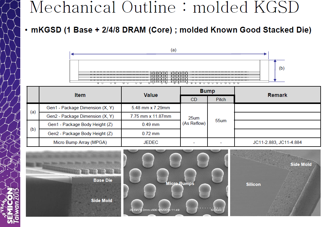
AMD was the first and only company to introduce products using HBM1. AMD's Radeon R9 Fury X GPUs featured 4 gigabytes of HBM1 using four 1 GB packages. Both AMD and Nvidia will introduce GPUs equipped with HBM2 memory this year. Samsung's first HBM2 packages will contain 4 GB of memory each, and the press release states that Samsung intends to manufacture 8 GB HBM2 packages within the year. GPUs could include 8 GB of HBM2 using half of the die space used by AMD's Fury X, or just one-quarter of the die space if 8 GB HBM2 packages are used next year. Correction: HBM2 packages may be slightly physically larger than HBM1 packages. For example, SK Hynix will produce a 7.75 mm × 11.87 mm (91.99 mm2) HBM2 package, compared to 5.48 mm × 7.29 mm (39.94 mm2) HBM1 packages.
The 4GB HBM2 package is created by stacking a buffer die at the bottom and four 8-gigabit (Gb) core dies on top. These are then vertically interconnected by TSV holes and microbumps. A single 8Gb HBM2 die contains over 5,000 TSV holes, which is more than 36 times that of a 8Gb TSV DDR4 die, offering a dramatic improvement in data transmission performance compared to typical wire-bonding based packages.
Samsung's new DRAM package features 256GBps of bandwidth, which is double that of a HBM1 DRAM package. This is equivalent to a more than seven-fold increase over the 36GBps bandwidth of a 4Gb GDDR5 DRAM chip, which has the fastest data speed per pin (9Gbps) among currently manufactured DRAM chips. Samsung's 4GB HBM2 also enables enhanced power efficiency by doubling the bandwidth per watt over a 4Gb-GDDR5-based solution, and embeds ECC (error-correcting code) functionality to offer high reliability.
TSV refers to through-silicon via, a vertical electrical connection used to build 3D chip packages such as High Bandwidth Memory.
Update: HBM2 has been formalized in JEDEC's JESD235A standard, and Anandtech has an article with additional technical details.
Previously:
AMD Teases x86 Improvements, High Bandwidth Memory GPUs
AMD Shares More Details on High Bandwidth Memory
Samsung Mass Produces 128 GB DDR4 Server Memory
Nvidia revealed key details about its upcoming "Pascal" consumer GPUs at a May 6th event. These GPUs are built using a 16nm FinFET process from TSMC rather than the 28nm processes that were used for several previous generations of both Nvidia and AMD GPUs.
The GeForce GTX 1080 will outperform the GTX 980, GTX 980 Ti, and Titan X cards. Nvidia claims that GTX 1080 can reach 9 teraflops of single precision performance, while the GTX 1070 will reach 6.5 teraflops. A single GTX 1080 will be faster than two GTX 980s in SLI.
Both the GTX 1080 and 1070 will feature 8 GB of VRAM. Unfortunately, neither card contains High Bandwidth Memory 2.0 like the Tesla P100 does. Instead, the GTX 1080 has GDDR5X memory while the 1070 is sticking with GDDR5.
The GTX 1080 starts at $599 and is available on May 27th. The GTX 1070 starts at $379 on June 10th. Your move, AMD.
NVIDIA is releasing the GeForce GTX 1080 Ti, a $699 GPU with performance and specifications similar to that of the NVIDIA Titan X:
Unveiled last week at GDC and launching [March 10th] is the GeForce GTX 1080 Ti. Based on NVIDIA's GP102 GPU – aka Bigger Pascal – the job of GTX 1080 Ti is to serve as a mid-cycle refresh of the GeForce 10 series. Like the GTX 980 Ti and GTX 780 Ti before it, that means taking advantage of improved manufacturing yields and reduced costs to push out a bigger, more powerful GPU to drive this year's flagship video card. And, for NVIDIA and their well-executed dominance of the high-end video card market, it's a chance to run up the score even more. With the GTX 1080 Ti, NVIDIA is aiming for what they're calling their greatest performance jump yet for a modern Ti product – around 35% on average. This would translate into a sizable upgrade for GeForce GTX 980 Ti owners and others for whom GTX 1080 wasn't the card they were looking for.
[...] Going by the numbers then, the GTX 1080 Ti offers just over 11.3 TFLOPS of FP32 performance. This puts the expected shader/texture performance of the card 28% ahead of the current GTX 1080, while the ROP throughput advantage stands 26%, and memory bandwidth at a much greater 51.2%. Real-world performance will of course be influenced by a blend of these factors, with memory bandwidth being the real wildcard. Otherwise, relative to the NVIDIA Titan X, the two cards should end up quite close, trading blows now and then.
Speaking of the Titan, on an interesting side note, NVIDIA isn't going to be doing anything to hurt the compute performance of the GTX 1080 Ti to differentiate the card from the Titan, which has proven popular with GPU compute customers. Crucially, this means that the GTX 1080 Ti gets the same 4:1 INT8 performance ratio of the Titan, which is critical to the cards' high neural networking inference performance. As a result the GTX 1080 Ti actually has slightly greater compute performance (on paper) than the Titan. And NVIDIA has been surprisingly candid in admitting that unless compute customers need the last 1GB of VRAM offered by the Titan, they're likely going to buy the GTX 1080 Ti instead.
The card includes 11 GB of Micron's second-generation GDDR5X memory operating at 11 Gbps compared to 12 GB of GDDR5X at 10 Gbps for the Titan X.
Previously: GDDR5X Standard Finalized by JEDEC
Nvidia Announces Tesla P100, the First Pascal GPU
Nvidia Unveils GTX 1080 and 1070 "Pascal" GPUs
JEDEC has announced that it expects to finalize the DDR5 standard by next year. It says that DDR5 will double bandwidth and density, and increase power efficiency, presumably by lowering the operating voltages again (perhaps to 1.1 V). Availability of DDR5 modules is expected by 2020:
You may have just upgraded your computer to use DDR4 recently or you may still be using DDR3, but in either case, nothing stays new forever. JEDEC, the organization in charge of defining new standards for computer memory, says that it will be demoing the next-generation DDR5 standard in June of this year and finalizing the standard sometime in 2018. DDR5 promises double the memory bandwidth and density of DDR4, and JEDEC says it will also be more power-efficient, though the organization didn't release any specific numbers or targets.
The DDR4 SDRAM specification was finalized in 2012, and DDR3 in 2007, so DDR5's arrival is to be expected (cue the Soylentils still using DDR2). One way to double the memory bandwidth of DDR5 is to double the DRAM prefetch to 16n, matching GDDR5X.
Graphics cards are beginning to ship with GDDR5X. Some graphics cards and Knights Landing Xeon Phi chips include High Bandwidth Memory (HBM). A third generation of HBM will offer increased memory bandwidth, density, and more than 8 dies in a stack. Samsung has also talked about a cheaper version of HBM for consumers with a lower total bandwidth. SPARC64 XIfx chips include Hybrid Memory Cube. GDDR6 SDRAM could raise per-pin bandwidth to 14 Gbps, from the 10-14 Gbps of GDDR5X, while lowering power consumption.
Samsung has announced the mass production of 16 Gb GDDR6 SDRAM chips with a higher-than-expected pin speed. The chips could see use in upcoming graphics cards that are not equipped with High Bandwidth Memory:
Samsung has beaten SK Hynix and Micron to be the first to mass produce GDDR6 memory chips. Samsung's 16Gb (2GB) chips are fabricated on a 10nm process and run at 1.35V. The new chips have a whopping 18Gb/s pin speed and will be able to reach a transfer rate of 72GB/s. Samsung's current 8Gb (1GB) GDDR5 memory chips, besides having half the density, work at 1.55V with up to 9Gb/s pin speeds. In a pre-CES 2018 press release, Samsung briefly mentioned the impending release of these chips. However, the speed on release is significantly faster than the earlier stated 16Gb/s pin speed and 64GB/s transfer rate.
18 Gbps exceeds what the JEDEC standard calls for.
Also at Engadget and Wccftech.
Related: GDDR5X Standard Finalized by JEDEC
DDR5 Standard to be Finalized by JEDEC in 2018
SK Hynix to Begin Shipping GDDR6 Memory in Early 2018
Samsung's Second Generation 10nm-Class DRAM in Production
Micron Spills on GDDR6X: PAM4 Signaling For Higher Rates, Coming to NVIDIA's RTX 3090
It would seem that Micron this morning has accidentally spilled the beans on the future of graphics card memory technologies – and outed one of NVIDIA's next-generation RTX video cards in the process. In a technical brief that was posted to their website, dubbed "The Demand for Ultra-Bandwidth Solutions", Micron detailed their portfolio of high-bandwidth memory technologies and the market needs for them. Included in this brief was information on the previously-unannounced GDDR6X memory technology, as well as some information on what seems to be the first card to use it, NVIDIA's GeForce RTX 3090.
[...] At any rate, as this is a market overview rather than a technical deep dive, the details on GDDR6X are slim. The document links to another, still-unpublished document, "Doubling I/O Performance with PAM4: Micron Innovates GDDR6X to Accelerate Graphics Memory", that would presumably contain further details on GDDR6X. None the less, even this high-level overview gives us a basic idea of what Micron has in store for later this year.
The key innovation for GDDR6X appears to be that Micron is moving from using POD135 coding on the memory bus – a binary (two state) coding format – to four state coding in the form of Pulse-Amplitude Modulation 4 (PAM4). In short, Micron would be doubling the number of signal states in the GDDR6X memory bus, allowing it to transmit twice as much data per clock.
[...] According to Micron's brief, they're expecting to get GDDR6X to 21Gbps/pin, at least to start with. This is a far cry from doubling GDDR6's existing 16Gbps/pin rate, but it's also a data rate that would be grounded in the limitations of PAM4 and DRAM. PAM4 itself is easier to achieve than binary coding at the same total data rate, but having to accurately determine four states instead of two is conversely a harder task. So a smaller jump isn't too surprising.
The leaked Ampere-based RTX 3090 seems to be Nvidia's attempt to compete with AMD's upcoming RDNA2 ("Big Navi") GPUs without lowering the price of the usual high-end "Titan" GPU (Titan RTX launched at $2,499). Here are some of the latest leaks for the RTX 30 "Ampere" GPU lineup.
Previously: GDDR5X Standard Finalized by JEDEC
SK Hynix to Begin Shipping GDDR6 Memory in Early 2018
Samsung Announces Mass Production of GDDR6 SDRAM
Related: PCIe 6.0 Announced for 2021: Doubles Bandwidth Yet Again (uses PAM4)
(Score: 0) by Anonymous Coward on Tuesday January 26 2016, @12:52AM
Graphics are used for gaming. And nothing else.
(Score: 0) by Anonymous Coward on Tuesday January 26 2016, @01:02AM
http://www.nvidia.com/object/drive-px.html [nvidia.com]
https://en.m.wikipedia.org/wiki/General-purpose_computing_on_graphics_processing_units [wikipedia.org]
http://www.top500.org/blog/beyond-beowulf-clusters-cores-and-a-new-era-of-top500/ [top500.org]
(Score: 0) by Anonymous Coward on Tuesday January 26 2016, @02:09AM
This could allow a PS4 or a PS4-Server model with 500+ gigabytes/sec of memory bandwidth. If they fixed the PS4 design to include ECC support, it would make an extremely fast processing node for any number of applications.
(Score: 3, Informative) by takyon on Tuesday January 26 2016, @05:48AM
Microsoft and Sony may offer a "mid-cycle refresh" for the Xbox One and PS4 consoles. Now that they are using AMD x86 chips, they could move to an improved version for lower power consumption, but more importantly, better performance to meet the needs of 4K and VR.
It's not like the hardware in these consoles is expensive anyway. But now that AMD is moving from the 28nm to the 14nm node, they could easily use a new 8-core chip with better capabilities. That's courtesy of the switch to x86.
The console cycle has typically been around 6-7 years. But they may offer a significant upgrade 3-4 years in this time around. For PS4, that probably means supporting new 4K Blu-ray discs [soylentnews.org] with capacities of 66 GB and 100 GB. Sony will also want to push their version of a VR headset at the time of the console refresh.
[SIG] 10/28/2017: Soylent Upgrade v14 [soylentnews.org]
(Score: 2) by Tork on Tuesday January 26 2016, @02:08AM
🏳️🌈 Proud Ally 🏳️🌈
(Score: 2) by meisterister on Wednesday January 27 2016, @01:33AM
I feel like I'm getting *whooshed* here.
Perhaps OP is being facetious?
(May or may not have been) Posted from my K6-2, Athlon XP, or Pentium I/II/III.
(Score: 3, Informative) by gman003 on Tuesday January 26 2016, @01:34AM
HBM2 blows GDDR5X out of the water, performance-wise. Should be easily twice as fast, maybe more depending on how fast they can clock it.
But, HBM2 will have a cost penalty. The interposer is claimed to cost about $30 more, and the fat memory controller uses up a good bit of die space, so it's only economical to do on big, expensive GPUs. So there will be plenty of room for GDDR5 in the market.
My guess is that the top GPU die will use HBM2 (so the top two or three models), followed by two dies using GDDR5, and then probably a die using DDR4 for the low-end. This goes for both AMD/Nvidia.
(Score: 2) by takyon on Tuesday January 26 2016, @01:50AM
The HBM cost calculation is interesting because it can also reduce the size of the GPU or other chip, reducing costs further (I'm not familiar with a problem with "fat memory controllers", and it's plain to see that AMD's Fury X was much smaller than previous flagship GPUs). I was a little mistaken on my calculations of the benefits of HBM2 over HBM1, but HBM1 reduced the area taken up by memory, and HBM2 will do the same:
4 GB per package HBM2 = 4 GB of memory in 91.99 mm2 (Hynix)
1 GB per package HBM1 = 4 GB of memory in 159.76 mm2 (Hynix)
Samsung will introduce an 8 GB HBM2 package around the end of 2016.
While AMD and Nvidia will be using HBM on GPUs, we will also see AMD using HBM on selected APUs (which apparently perform much/somewhat better given good memory bandwidth) as well as a version of Intel's Xeon Phi (not sure which ones).
[SIG] 10/28/2017: Soylent Upgrade v14 [soylentnews.org]
(Score: 2) by Hairyfeet on Tuesday January 26 2016, @02:06AM
Yeah with AMD's APUs bandwidth is king, I've gotten a nearly 30% speed boost just by going up a couple notches in RAM speed. the AMD APUs are really powerful chips, with plenty of vids of AAA titles like BF4 playing great on them but they are ultimately bottlenecked by the RAM speed. If AMD can pair their APUs with say a Gb of HBM to supplement a couple GB of system memory? They should be quite awesome for budget gaming rigs.
ACs are never seen so don't bother. Always ready to show SJWs for the racists they are.
(Score: 2) by takyon on Tuesday January 26 2016, @02:22AM
30%? Damn that's a lot. I'm guessing you moved from 1333 to 1866 MHz.
The information about AMD APUs with HBM is very tentative.
http://wccftech.com/evidence-amd-apus-featuring-highbandwidth-stacked-memory-surfaces/ [wccftech.com]
http://wccftech.com/xbox-one-may-be-getting-a-new-apu-based-on-amds-polaris-architecture/ [wccftech.com]
http://www.kitguru.net/components/apu-components/matthew-wilson/amd-said-to-be-working-on-zen-apu-with-hbm/ [kitguru.net]
http://hexus.net/tech/news/cpu/89246-zen-based-apu-hbm-amd-carrizo-successor/ [hexus.net]
(Notice I linked only rumor-tier sites. Here's an Anandtech [anandtech.com] bit:)
Zen could be a terrific advance for AMD. I am in the market for laptops in the $300-$800 range, which I consider to offer the best bang for the buck (better screen resolutions and even some discrete graphics at the top-end of that range).
Zen promises to deliver a 40% increase in IPC (compare to recent 2-10% increases per Intel generation) and does away with the Bulldozer/Excavator CMT modules. Yet maybe they will still offer up to 8 cores on some Zen chips... if AMD delivers on everything, we could see chips that are not only the best price/performance but even outperform top-end Intel. Let me just copy and paste some text I wrote elsewhere:
[SIG] 10/28/2017: Soylent Upgrade v14 [soylentnews.org]
(Score: 2) by Hairyfeet on Tuesday January 26 2016, @07:14AM
Well a LOT of laptops come with frankly crap memory so yeah kicking it up a couple notches really helps.
and just FYI I try to avoid Anandtech, because if you turn off your adblock? Its all Intel ads. I've even read articles where the author admitted that most new triple A titles require a quad core and then promptly recommended an i3 over an FX6300 for a gaming PC!
As for Zen? The fact that they lured back the guy that designed the Athlon64 has peaked my curiosity, the Athlon64 was a revolutionary chip and after leaving AMD he ended up designing many of the chips used in the Apple mobile devices so the guy hasn't been just sitting on ass getting rusty. That said as I've argued before frankly PCs went from "good enough" to insanely overpowered several years back and unless that new chip comes with a new way of programming to back it up or somehow causes the MHz race to start back up? I just don't know how much of a difference its gonna make. I mean I've got plenty of gaming customers out there still running C2Q and Phenom IIs and paired with a decent GPU they are getting great framerates with plenty of bling and I know I'm deliriously happy with my FX-8320E and I really don't see any programs or games coming down the pipe that is gonna need more than 8 cores (hell most don't even take advantage of 4) or more than 4GHz of speed.
Where this CAN make a pretty big splash would be in the laptop and budget gaming space as you noted, plenty of folks I know would love a laptop that was decent at gaming but the prices are just too high, if they can come out with a good gaming APU that can be put in a laptop for sub $450 while making a decent profit? That thing is gonna sell. I'm also seeing a lot more go for the APUs for budget gaming rigs simply because you can build a sub $400 system that can play games like BF4 at 30FPS+ and even if they have to raise the price by say $50-$75 if they can get performance equal to or greater than a current $120 card like the 750ti? These might really take off.
The final thing is getting rid of FM2+ and AM3+ for AM4, while it means I won't be able to upgrade down the line (I already got 8 cores and 16Gb of RAM, I'm really not worried) but if the rumors are true that both desktop and mobile will use the same AM4 socket? We could see something we haven't seen since the days of the 386, user upgradable laptops which would frankly be awesome. Even if its not easy for the user to swap i could see the OEMs liking this as it'll mean they can keep a laptop design in production and simply upgrade the APU as new models come out to keep the system fresh, as well as easily allowing the same unit to be sold for different prices points by simply swapping chips, VERY cool.
ACs are never seen so don't bother. Always ready to show SJWs for the racists they are.
(Score: 2) by takyon on Tuesday January 26 2016, @08:20AM
Computers may be "good enough" but AMD certainly has room to improve.
It has done well with the integrated graphics APU and we should see that continue. Skylake is supposedly a huge improvement, but the best Skylake "Iris Pro" 580 integrated graphics, GT4e, is nowhere to be found. The 'e' stands for eDRAM [wikipedia.org].
Oh, I guess they have gone on a publicity blitz for Iris Pro 580 / GT4e in the weeks since CES. They are saying it's a discrete graphics killer! And it might be for that (higher end?) budget segment. Luckily VR and 1440p/4K/5K/8K leaves open the "need" for better GPUs. Especially if any of that is desired on laptops or mobile devices.
http://wccftech.com/intel-skull-canyon-nuc-iris-pro-580-powerful-2016/ [wccftech.com]
http://wccftech.com/intel-iris-pro-graphics-gamers/ [wccftech.com]
They suggest that GT4e is better than what AMD has out on the market right now. I don't doubt that, but AMD's move to 14nm will give it plenty of room to improve their own integrated graphics. GT4e chips are also likely to be very expensive. While we have heard plenty about Zen's 40% increase in IPC (which could be misleading in some way), we don't know anything about Zen's integrated graphics. Theoretically, reducing transistors from 28nm to 14nm could mean 4 times the area (2x2)! Yeah, I know that's not actually true.
Back to improving chips. AMD needs to lower power consumption. Intel's recent Core-M chips are approaching the power consumption of its lower performance Atom chips, though they are much more expensive. Some of these lower-powered CPU brands may merge in the future. Like Atom and Celeron. Fanless laptops are great. I'm using an Intel Celeron N2830 based Chromebook. That has a TDP of 7.5 W, probably within reach of AMD. Let's see a 14nm AMD chip that can be put in a fanless tablet, laptop, or ultrabook. Ok so they do have [wikipedia.org] 4.5 Watt "Mullins" but they seem to be smoked by Intel Core-M. Compare E1 Micro-6200T to Core M-5Y10.
While you're right that core counts don't need to increase much, 8 core is a good milestone to reach. It future proofs the system and allows many applications/processes/tabs to run simultaneously. Also, both the Xbox One and PS4 are using 8-core x86 AMD "Jaguar" chips. While 1 of those cores aren't available to game developers, on the PS4 side, Sony has recently unlocked [wired.co.uk] the 7th core [extremetech.com]. So game developers have 6-7 cores to work with on millions of consoles. They may not be beefy cores, but it means we will see more parallelism in gaming. With the x86 architecture shared between consoles and PCs, you will see multi-platform games that can readily (hopefully?) take advantage of more than 4 cores. Productivity applications, video editing/encoding, servers, etc. can usually take advantage of additional cores.
Since Intel has frozen the core count at 4 for mainstream chips (6 and 8 for Sandy Bridge-E and Haswell-E), AMD could try and pull ahead in some benchmarks with new hex- and octo-core chips. They claimed to have made 6 and 8 core chips with the introduction of Bulldozer, but the dual-core "modules" were such a lie that they are being sued over it [theregister.co.uk]. Now that they are switching from Clustered Multithreading to Simultaneous Multithreading, Zen will probably include what can be considered "real" cores. They will probably make 6 and 8 core mainstream Zen models, although their mobile chips have been limited to quad-core (two modules).
[SIG] 10/28/2017: Soylent Upgrade v14 [soylentnews.org]
(Score: 2) by Hairyfeet on Tuesday January 26 2016, @09:00AM
In what way, other than benches where I can produce article after article where Intel or the benchmarking company was caught rigging? Trusting benches anymore is about like the old "Quack.exe" on the bullshit scale.
To me a MUCH better metric is real life...can you name a single game that won't play on an FX-6300, a chip commonly found for sub $99? Or even the Athlon FM2 quad which goes for $79 and is recommended in many articles as the basis for budget gaming boxes? Lets face it, software, even games, just hasn't kept up with CPUs in a loooong time, and with the "next gen" consoles both using AMD netbook chips? I really do not see that changing. I used to have a buddy at the state capital that had a blind A/B test set up on a desk just to deal with those "AMD Suxors lulz" gaming tards where he had a $300 i5 on one side and a $99 FX-6300 on the other with both having $150 mainstream GPUs...know what anybody that tried it found? You literally could not tell the difference when it came to real world applications and games, the difference was so slight it was below the margin for error. Hell he could have easily swapped the FX for a Phenom II and I still doubt anybody would have known as for years I had a customer running high end GPU accelerated CAD designing robots and rockets to help out the local college on its NASA entries and it was all being done on a fricking Phenom I quad!
This is why I worry that AMD will end up coming out with the superior chip and we will see the Pentium 4 all over again, remember that? Intel had a clear dog on its hands yet it dominated the market because it rigged benches and paid off OEMs. The "2 billion" AMD settlement wasn't even 5% of what they made during that period so that obviously won't be a deterrent and the DOJ has been toothless for over a decade. This is why I've said for years AMD is doing it wrong because the first rule of business is you do NOT play the other guy's game, you make him play yours! I learned that lesson the hard way, by picking through the remains of other shops that all went broke trying to compete with Dell on price, did I do that shit? Fuck no! I instead pointed out that service from Dell was shit, it was filled with crapware, and would THEY come out to your house and set the system up for you at no extra charge? Nope.
For AMD to get ahead they need to stop trying to play the numbers game with Intel and instead show off what their chips can DO and how much you can save while doing itg. Show their laptops playing killer games while the Intel shit GPUs struggle while costing 40%+ more for the same hardware, show 2 systems built for $700 and how much nicer you get if you went AMD, with more RAM, SSD, dedicated GPU, etc. this strategy WORKS because we have proof, look at Nintendo SNES versus Genesis where in pure processing power the SNES had better hardware but Sega cleaned up because they refused to play the numbers game Nintendo's way, instead pushing how many cool games they could offer and how cool they looked.
So whether Zen is the second coming or not its really gonna depend on AMD not playing Intel's game. They have a pretty big advantage when it comes to GPUs and HBM should make it that much bigger of a gap but if they refuse to do anything but play the game by Intel's rules? They are gonna lose.
ACs are never seen so don't bother. Always ready to show SJWs for the racists they are.
(Score: 2) by meisterister on Wednesday January 27 2016, @01:52AM
They are saying it's a discrete graphics killer!
Aaand they said that for Broadwell, Haswell, Ivy Bridge, Sandy Bridge, Westmere, and, while not really fair because it is itself a discrete graphics solution with some weird integrated graphics-like features, the i740.
(May or may not have been) Posted from my K6-2, Athlon XP, or Pentium I/II/III.
(Score: 2) by gman003 on Tuesday January 26 2016, @03:12PM
At the moment, sure. Last year they had a big AMD sponsorship, to the point that they had an actual AMD section, styled in AMD red. Under neither sponsorship did I find much bias, outside the comments section. For example, if you look at their recent reviews for AMD's A8-7670K [anandtech.com], the review boils down to "AMD still has problems with CPU performance, but if you want to game on a budget, it works great", so they're not being unfair to AMD. And they're honestly reporting on Intel's supply issues [anandtech.com], so they aren't helping Intel on that front either.
As for the i3 vs. FX6300, neither of them are true quad-cores. Intel, in an uncharacteristic bit of honesty, makes a clear distinction between hardware cores and logical threads. AMD gave their logical threads a bit more dedicated hardware, but they used that to call it a full core, and then call the actual core a "module" (ever wonder why there are no "triple-core" FX chips, like there were in the Phenom II days? It's because it's physically impossible). I could quibble about semantics all day, but instead I'll just refer you to benchmarks - any set of benchmarks, really, will show that the FX6000s benchmarks in the same region as the two-cores-hyperthreaded i3s, not the quad-core i5s. At this point, it might be worth it to grab the i3 just for the wider range of motherboards to choose from, plus the more modern chipset, particularly if you can grab it for a similar price.
(Score: 2) by gman003 on Tuesday January 26 2016, @03:43AM
HBM makes the memory chips themselves take up less space, but a memory controller that can run a 4096-bit memory bus is going to be large by its very nature.
And while the Fury X and Fury Nano were small cards, the actual GPU on them was massive. Nearly 600mm^2, and that's not including the interposer. Since the biggest factor in the cost to manufacture a chip is the physical size, this of course made the actual GPU quite expensive.
(Score: 2) by takyon on Tuesday January 26 2016, @04:18AM
Yeah I guess you're right.
http://www.anandtech.com/show/9390/the-amd-radeon-r9-fury-x-review/3 [anandtech.com]
Perhaps the move from 28nm to 14nm will shave off 10-20% off the size.
[SIG] 10/28/2017: Soylent Upgrade v14 [soylentnews.org]